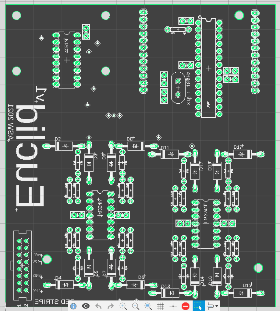
Next up was the logic board – the one containing all of the ICs. There were no particular layout requirements for this board other than the positioning of the header pins at the top and the large screw holes, so I tried a few different iterations of component placements before settling on the one shown here. Once again, I used the top half of the board for power and put signals on the bottom half, although this time a few vias were needed for power, as there were not just +5V and GND to consider, but also +12V and -12V.
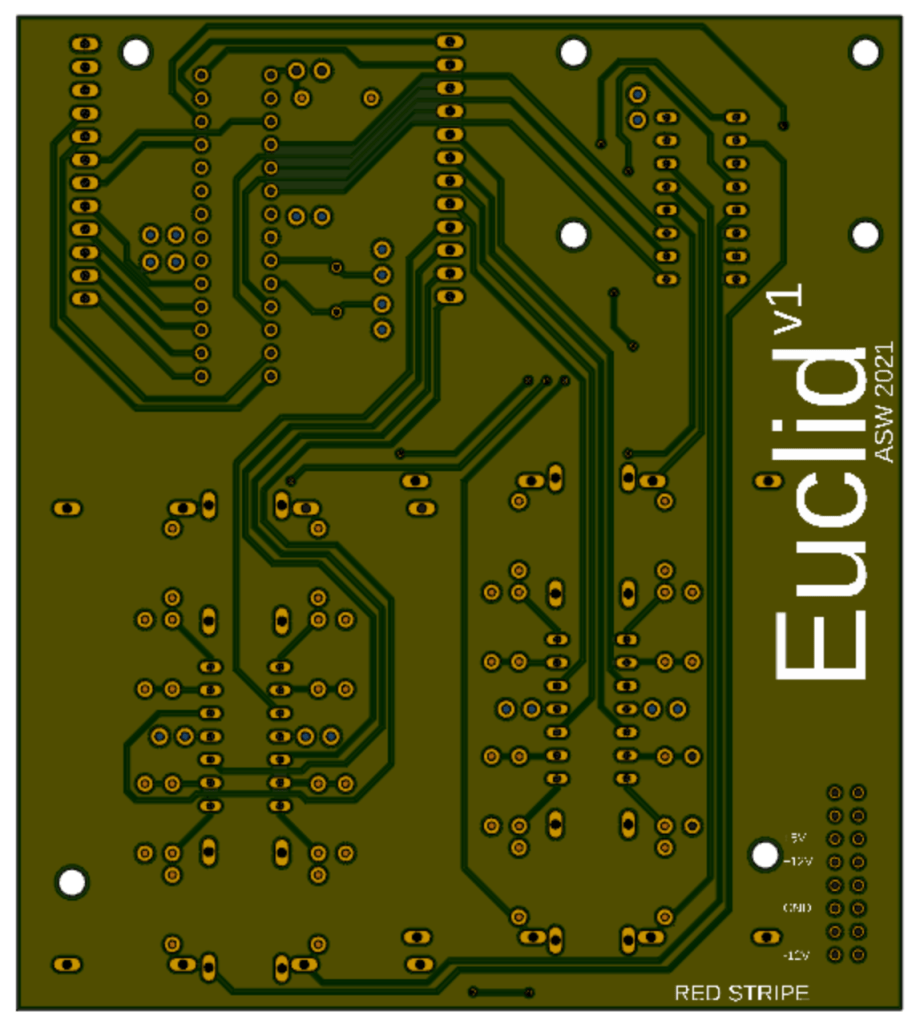
This time I could not change the positions of the header pins to simplify routing, as these were already set by the first board design, but I could reorder which ATMEGA pins were used for which I/O, so most of these will need to be tweaked in my code. I added silkscreen to the back of this board, with the module name and version number, as well as a few reminders about the power connector’s polarity. I am pretty happy with my routing on this board – I just hope that it all works when it arrives!

